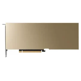
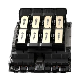
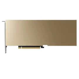
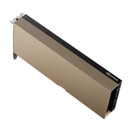
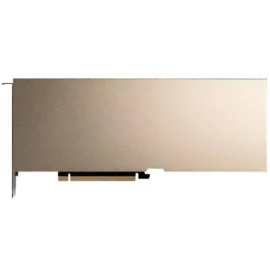
The NVIDIA H200 GPU is the latest addition to NVIDIA’s cutting-edge lineup of GPUs, marking a significant step forward in performance and efficiency. Powered by NVIDIA’s next-generation Hopper architecture, the H200 is designed to meet the growing demands of artificial intelligence (AI), machine learning, and high-performance computing (HPC) applications. Let’s dive deeper into what makes the NVIDIA H200 an exceptional choice for professionals.
Table of Contents
ToggleWhat is the H200 GPU?
The NVIDIA H200 GPU is a state-of-the-art graphics processing unit tailored for advanced computational tasks. As part of NVIDIA’s new Hopper architecture, it excels in AI model training, inferencing, and complex data processing. This GPU builds on the success of its predecessor, the NVIDIA H100, offering enhanced performance, improved power efficiency, and superior scalability.
Engineered for data centers and enterprise workloads, the H200 GPU is designed to handle the demands of cutting-edge technologies like generative AI and real-time analytics.
NVIDIA H200 Price
The price of NVIDIA AI chips can vary widely depending on the market. Below is an approximate price range. The H200 is an advanced AI and machine learning GPU, offering top-tier performance. Pricing for the H200 starts at around $22,000, with variations depending on the specific memory configuration and market conditions.
NVIDIA H200 Specs & Benchmark
Technical Specifications sourced from NVIDIA official site:
| Technical Specifications | H200 SXM | H200 NVL |
| FP64 | 34 TFLOPS | 30 TFLOPS |
| FP64 Tensor Core | 67 TFLOPS | 60 TFLOPS |
| FP32 | 67 TFLOPS | 60 TFLOPS |
| TF32 Tensor Core* | 989 TFLOPS | 835 TFLOPS |
| BFLOAT16 Tensor Core* | 1,979 TFLOPS | 1,671 TFLOPS |
| FP16 Tensor Core* | 1,979 TFLOPS | 1,671 TFLOPS |
| FP8 Tensor Core* | 3,958 TFLOPS | 3,341 TFLOPS |
| INT8 Tensor Core* | 3,958 TFLOPS | 3,341 TFLOPS |
| GPU Memory | 141GB | 141GB |
| GPU Memory Bandwidth | 4.8TB/s | 4.8TB/s |
| Decoders | 7 NVDEC, 7 JPEG | 7 NVDEC, 7 JPEG |
| Confidential Computing | Supported | Supported |
| Max Thermal Design Power (TDP) | Up to 700W (configurable) | Up to 600W (configurable) |
| Multi-Instance GPUs | Up to 7 MIGs @ 18GB each | Up to 7 MIGs @ 16.5GB each |
| Form Factor | SXM | PCIe |
| Interconnect | NVIDIA NVLink: 900GB/s, PCIe Gen5: 128GB/s | 2- or 4-way NVIDIA NVLink bridge: 900GB/s per GPU, PCIe Gen5: 128GB/s |
| Server Options | NVIDIA HGX™ H200 partner and NVIDIA-AI Certified Systems™ with 4 or 8 GPUs | NVIDIA MGX™ H200 NVL partner and NVIDIA-Certified Systems with up to 8 GPUs |
| NVIDIA AI Enterprise | Add-on | Included |
Note: The asterisk (*) indicates specifications with sparsity
What is the Difference Between H100 and H200 GPU?
As the successor to the H100, the H200 pushes the boundaries further with enhanced performance and capabilities. When compared to the H100, the key difference comes in the massive increase in VRAM, with 141GB of HBM3e memory offering a substantial upgrade to the H100’s 80GB HBM3. The H200 is capable of 43% higher GPU memory bandwidth than the H100, with a peak of 4.8TB/s and 900GB/s of P2P bandwidth.
H100 GPU Technical Specifications sourced from NVIDIA official site:
| Technical Specifications | H100 SXM | H100 NVL |
| FP64 | 34 teraFLOPS | 30 teraFLOPS |
| FP64 Tensor Core | 67 teraFLOPS | 60 teraFLOPS |
| FP32 | 67 teraFLOPS | 60 teraFLOPS |
| TF32 Tensor Core* | 989 teraFLOPS | 835 teraFLOPS |
| BFLOAT16 Tensor Core* | 1,979 teraFLOPS | 1,671 teraFLOPS |
| FP16 Tensor Core* | 1,979 teraFLOPS | 1,671 teraFLOPS |
| FP8 Tensor Core* | 3,958 teraFLOPS | 3,341 teraFLOPS |
| INT8 Tensor Core* | 3,958 TOPS | 3,341 TOPS |
| GPU Memory | 80GB | 94GB |
| GPU Memory Bandwidth | 3.35TB/s | 3.9TB/s |
| Decoders | 7 NVDEC, 7 JPEG | 7 NVDEC, 7 JPEG |
| Max Thermal Design Power (TDP) | Up to 700W (configurable) | 350-400W (configurable) |
| Multi-Instance GPUs | Up to 7 MIGs @ 10GB each | Up to 7 MIGs @ 12GB each |
| Form Factor | SXM | PCIe dual-slot air-cooled |
| Interconnect | NVIDIA NVLink: 900GB/s, PCIe Gen5: 128GB/s | NVIDIA NVLink: 600GB/s, PCIe Gen5: 128GB/s |
| Server Options | NVIDIA HGX H100 Partner and NVIDIA-Certified Systems™ with 4 or 8 GPUs | Partner and NVIDIA-Certified Systems with 1–8 GPUs |
| NVIDIA Enterprise | Add-on | Included |
Note: The asterisk (*) indicates specifications with sparsity
Benchmark results for the H200 GPU highlight its unparalleled performance. Early tests show that it outperforms the H100 in tasks like large-scale AI model training, data processing, and scientific simulations. The improved H200 GPU memory and enhanced CUDA core design contribute significantly to these benchmarks.
The NVIDIA H200 PCIe variant is expected to deliver exceptional results for diverse workloads, allowing seamless scaling in multi-GPU setups. Additionally, its reduced NVIDIA H200 power consumption enables enterprises to achieve greater performance-per-watt efficiency.
The NVIDIA H200 is not just another GPU; it is a technological marvel aimed at setting new benchmarks in AI and HPC. Whether you’re an enterprise looking to NVIDIA H200 buy or an enthusiast comparing NVIDIA H200 vs H100, this GPU promises to redefine possibilities in computing. Keep an eye on its official release to experience the future of GPU technology.

